Research
Microstructure heterogeneity in metal AM: A double edged sword!

Since its inception, additive manufacturing (AM) has been synonymous with near-net-shape manufacturing. The ability to build components with complex geometry has inspired novel designs of metallic parts across the biomedical, aerospace, and automotive industries. The disruptive potential of AM, however, goes beyond complexity of shape. Because the material is formed point by point at a microscopic scale following non-equilibrium processes, AM provides the capability of producing metal parts with complex, heterogeneous microstructures that are not attainable via traditional manufacturing routes. Until now, this unique feature has been regarded as deleterious for industrial applications because uncontrolled microstructure heterogeneity yields large property scatter across otherwise identical parts, casting uncertainty over their lifetime and performance (see figure on the right).

However, “taming” the microstructure heterogeneity offered by AM would unlock the design and production of materials with superior and more predictable properties by arranging dissimilar microstructures into complex 3D architectures as if they were pieces of a LEGO brick construction set (see figure on the left). Our goal at the AddME Lab is to understand and control this microstructure heterogeneity to design and produce novel materials with superior properties and more predictable behavior. Our vision is that this unique capability will enable a new design paradigm in metal AM for producing both geometry- and microstructure-optimized parts.
Starting from powders

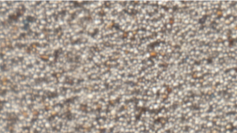
Because AM spans over six orders of magnitude in length scale—from melt pools that are tens of microns in width to meter-long builds—microstructural heterogeneities and defects are prone to be incorporated ubiquitously, layer by layer, throughout the entire build volume. Using our proprietery powder bed scanner (PBS) technology, we investigate the causes that yield to part inconsistency and property scatter as early as at the powder recoater step. The PBS combines a flatbed document-scanner sensor with the re-coater arm of a LPBF machine. Employing this technology during powder bed fusion processes allows assessing the powder layer quality and surface topography of the selectively melted regions in-situ, layer by layer, to a remarkable spatial resolution of ~5 μm and over the entire build area (see figure on the right). Correlating this information with the post-mortem analysis of defects (such as porosity) and microstructural inhomogeneities may provide insights into the origins of materials variability in AM and inspire new strategies to mitigate it during processing. The PBS can also be used to monitor powder contamination in-situ, during AM processes, to quantify oxygen uptake and estimate the "age" of the powders (i.e., how many times it can be used before being disposed). This information may be used to devise more efficient powder recycling routines in industry.
High-Throughput Microstructure Analysis

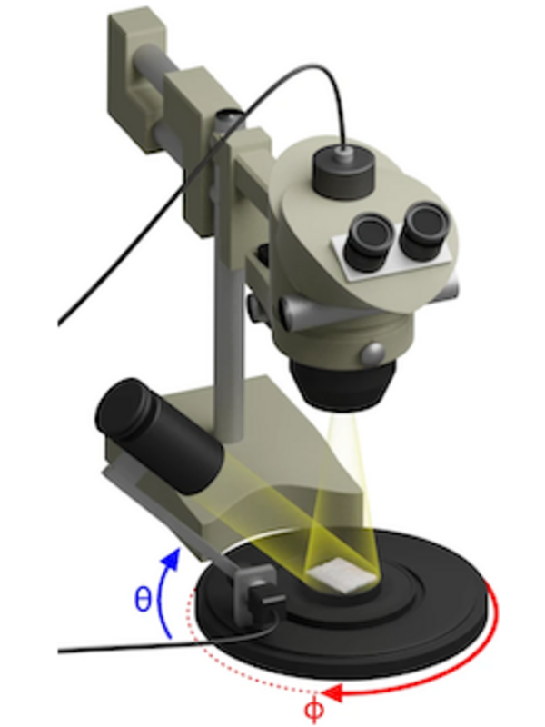
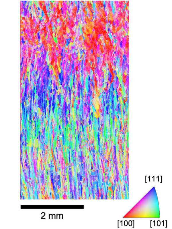
While high-energy X-ray and electron diffraction techniques are essential to investigate the solidification process and the local microstructure of AM alloys, their low throughput and limited field of view prevent their use to assess the large-scale microstructure heterogeneity found in these materials (exemplified in the top figure in this page). For this reason, we use a technique of our invention called directional reflectance microscopy (DRM)to perform large-scale microstructure analysis of AM parts (see figure on the left). DRM is entirely based on optical microscopy and provides grain orientation mapping capabilities on chemically-etched solids by correlating optical surface reflectance to the local atomic lattice orientation. With DRM, we can map grain orientation on metals, ceramics, composites, and even multi-phase metal alloys. The two orientation maps above were actually produced using DRM! At the AddME Lab, we belive that DRM will ease the characterization of microstructure heterogeneity in AM parts and provide an invaluable tool to establish processing-structure-property relationships for AM alloys.
Microstructure Control during Metal AM

The steep, local thermal gradients, and rapid cooling rates typical of fusion-based AM processes yield microstructures with large residual stresses, site-specific elemental partitioning, and directionally grown crystals. These features have a direct impact on the homogeneity of the microstructureand the mechanical anisotropy of the alloy. By investigating the local solidification conditions in different alloys as a function of AM process parameters, we devise novel AM strategies to tailor such microstructural features to a high level of detail. We have demonstrated the ability to form quasi-single crystals by controlling the laser scanning direction, and have used it to make our own pseudo-polycrystals which do not even exist in nature (See QR code above and the helicoidal crystal on the right). We are also studying how the solidification structure affects the recrystallisation behaviour of engineering alloys. Gaining control over it would enable engineering the grain structure and the grain boundary character distribution of these materials.
Heterogeneous Microstructures for Multifunctional Materials
Understanding microstructure formation in fusion-based AM processes, the causes that lead to microstructure heterogeneity, and how these AM microstructures affect parts properties and performance offer the opportunity to design multifunctional materials that integrate dissimilar textures, phases, grain boundary networks, and grain structures within the same build at a high spatial resolution. Such materials could easily outperform their conventionally-manufactured counterparts by combining properties that appear mutually exclusive, such as strength and toughness. Research is ongoing at the AddME Lab to investigate the mechanical behaviour of the complex microstructures we synthesize and identify intelligent ways to combine them into optimized "microstructure architectures". Stay tuned for more on that front!
